
.png)
Characteristics of Light Source of Communication
To be useful in an optical link, a light source needs the following characteristics:
1. It must be possible to operate the device continuously at a variety of temperatures for
many years.
2. It must be possible to modulate the light output over a wide range of modulating
frequencies.
3. For fiber links, the wavelength of the output should coincide with one of transmission windows for
the fiber type used.
4. To couple large amount of power into an optical fiber, the emitting area should be small.
5. To reduce material dispersion in an optical fiber link, the output spectrum should be
narrow.
6. The power requirement for its operation must be low.
Light Emitting Diode (LED)
LED stands for Light Emitting Diode, which is a type of semiconductor device that emits light when a current flows through it. LEDs work based on a process called electroluminescence, which is the emission of light from a material when an electric current is passed through it.The basic structure of an LED consists of a semiconductor material, such as gallium arsenide, which has been doped with impurities to create a p-n junction. The p-n junction acts as a one-way valve for the flow of electrons, allowing current to flow in one direction but not the other.
When a forward voltage is applied to the p-n junction, electrons from the n-type region and holes from the p-type region combine at the junction, releasing energy in the form of photons. The energy of the photons corresponds to the bandgap of the semiconductor material, which determines the color of the emitted light.
The intensity of the light emitted by an LED is directly proportional to the current flowing through it, up to a certain point called the maximum current. Beyond this point, the LED can be damaged or destroyed.
.png)
Advantages of LED:
1.Simpler fabrication There are no mirror facets and in some structures no stripedgeometry.
2. Cost The simpler construction of the LED leads to much reduced cost which is always likely to be
maintained.
3. Reliability The LED does not exhibit catastrophic degradation and has proved far less sensitive to gradual
degradation than the injection laser. It is also immune to self-pulsation and modal noise problems.
4. Generally less temperature dependence The light output against current characteristic is less affected by
temperature than the corresponding characteristic for the injection laser. Furthermore, the LED is not a threshold
device and therefore raising the temperature does not increase the threshold current above the operating point and
hence halt operation.
5. Simpler drive circuitry This is due to the generally lower drive currents and reducedtemperature dependence
which makes temperature compensation circuits unnecessary.
6. Linearity. Ideally the LED has a linear light output against current characteristic
This can prove advantageous where analog modulation is concerned.
Drawbacks:
(a) Generally lower optical power coupled into a fiber (microwatts).
(b) Usually lower modulation bandwidth.
(c) Harmonic distortion.
LED structures
There are two main types of LED structures:Homojunction LED: In a homojunction LED, the p-type and n-type semiconductor layers are made of the same material, usually gallium arsenide (GaAs). The p-n junction is formed by doping the semiconductor material with impurities such as silicon or zinc. When a forward voltage is applied to the p-n junction, electrons and holes recombine, releasing energy in the form of light.
Heterojunction LED: In a heterojunction LED, the p-type and n-type semiconductor layers are made of different materials, such as gallium arsenide and aluminum gallium arsenide (AlGaAs). The different materials have different bandgap energies, which allow for more efficient electron and hole recombination, resulting in brighter light. Heterojunction LEDs also have a wider range of colors and are more efficient than homojunction LEDs.
Double Heterojunctions
Double Heterojunctions (DH)
In order to achieve efficient confinement of emitted radiation double heterojunctions are used
in LED structure. A heterojunciton is a junction formed by dissimilar semiconductors. Double
heterojunction (DH) is formed by two different semiconductors on each side of active region.

Surface Emitting LEDs
It is modified form of DH LED (Double Heterojunction LED). In this LED type, optical fiber is butt-coupled with itself.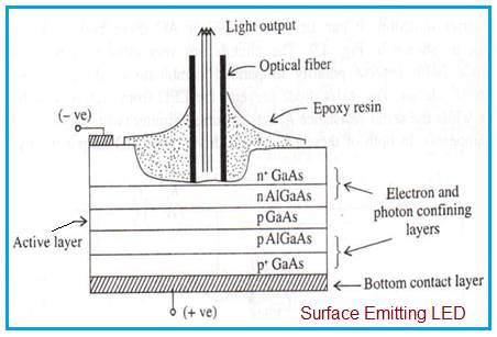
• The surface emitting LED structure consists of thin central active layer of p type GaAs.
• This central layer is bounded by n-type AlGaAs/n+-type GaAs at the top side.
• This central layer is bounded by p-type AlGaAs/p+-type GaAs at the bottom side.
• The extreme top n+ type GaAs and bottom p+-type GaAs layers are used to provide low resistive ohmic contacts only.
• The external optical fiber is butt connected by etching the top layers and by shielding with epoxy resin.
• When refractive indices of both p-type and n-type materials are same, light is free to come out from all the sides of the semiconductor device due to no confinement. However only active region near the surface will emit the significant amount of light while absorbing from the other parts. Hence it is known as surface emitting LED.
• Maximum optical power Pc is coupled with the optical fiber is expressed as follows.
• Pc = π * (1-R) * A* Rs * (NA)2
Where,
R = Reflection loss at fiber surface
A = Fiber cross section area
Rs = Radiance amount from source
NA = Numerical Aperture
Benefits or advantages of Surface Emitting LED
1. Optical coupling coefficient of LED with external fiber system is relatively higher. Hence this LED offers high optical coupling efficiency.2. Optical loss (due to internal absorption) is very low. This is because of carrier recombination near its top heterojunction.
3. InP/InGaAsP based LED is used for long wavelength applications.
It offers higher efficiency with low to high radiance.
4. The top n-GaAs contact layer ensures low thermal resistance and contact resistance. This allows high current densities and high radiation intensity.
5. The internal absorption in the device is very low due to larger bandgap confining layers. Moreover reflection coefficient at the back crystal face is high which gives good forward radiance.
Drawbacks or disadvantages of Surface Emitting LED
1. The surface emitting LED can transmit data rate less than 20 Mbps than edge emitting LED.2. It contains short optical link with large NA (Numerical Aperture).
Edge-emitting LED
.png)
The edge emitter consists of an active pn junction region
where the photons are generated and two light-guiding layers that function in
the same manner as an optical fiber. This structure forms a waveguide channel
that directs the optical radiation toward the edge of the device, where it can be
coupled into an optical fiber. The emission pattern of the edge emitter is more
directional than that of a surface emitter, which allows a greater percentage of
the emitted light to be coupled into a fiber.
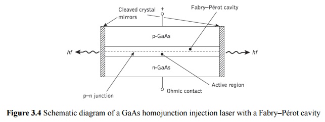
Semiconductor Injection Laser
Stimulated emission by the recombination of the injected carriers is encouraged in the semiconductor injection
laser (also called the injection laser diode (ILD) or simply the injection laser) by the provision of an optical
cavity in the crystal structure in order to provide the feedback of photons. This gives the injection laser several
major advantages over other semiconductor sources (e.g. LEDs) that may be used for optical communications.
These are as follows:
1. High radiance due to the amplifying effect of stimulated emission. Injection lasers will generally supply mill
watts of optical output power.
2. Narrow line width on the order of 1 nm (10 Å) or less which is useful in minimizing the effects of material
dispersion.
3. Modulation capabilities which at present extend up into the gigahertz range and will undoubtedly be
improved upon.
4. Relative temporal coherence which is considered essential to allow heterodyne (coherent) detection in high capacity systems, but at present is primarily of use in single-mode systems.
5. Good spatial coherence which allows the output to be focused by a lens into a spot which has a greater
intensity than the dispersed unfocused emission.
Advantages of Laser Diode
Simple economic design.
High optical power.
Production of light can be precisely controlled.
Can be
used at high temperatures.
Better modulation capability.
High coupling efficiency.
Low spectral width (3.5 nm)
Ability to transmit optical output powers between 5 and 10 mW.
Ability to
maintain the intrinsic layer characteristics over long periods.
Disadvantages of Laser Diode
At the end of fiber, a speckle pattern appears as two coherent light beams add or subtract their
electric field depending upon their relative phases.
Laser diode is extremely sensitive to overload currents and at high transmission rates, when
laser is required to operate continuously the use of large drive current produces unfavourable
thermal characteristics and necessitates the use of cooling and power stabilization.
Comparison of LED and Laser Diode
| PARAMETERS | LED | LASER |
|---|---|---|
| Working Principle | Electro-luminance | Stimulated Emission |
| Full Form | Light Emitting Diode | Light Amplification by Stimulated Emission of Radiation |
| Response | Slow Response | Fast response in comparison to LED |
| Driving Current | It ranges from 50 to 100 mA. | It ranges from 5 to 40 mA. |
| Nature of Emitted Light | Incoherent and consists of various colours. | Coherent and Monochromatic. |
| Junction Area during Manufacturing | Wide Junction Area | Narrow and small Junction |
| Bandwidth Range | It lies in the range of 10 to 50 THz. | It lies in the narrow range i.e. from 1 MHz to 2 MHZ. |
| Power to light Conversion Efficiency | Approx 20 % | Approx 70 % |
| Numerical Aperture of the obtained Light Beam | Higher in LEDs | Extremely low as compared to LEDs. |
| Cost | Low cost and thus economical. | High cost and thus used in the specific application. |
Principles of Optical Detectors
The photodetector works on the principle of optical absorption. The main requirement
of light detector or photodetector is its fast response. For fiber optic communication
purpose most suited photodetectors are PIN (p-type- Instrinsic-n-type) diodes and APD
(Avalanche photodiodes)
The performance parameters of a photodetector are responsivity, quantum
efficiency, response time and dark current.
PIN diode
A simple way to increase the depletion-region width is to insert a layer of undoped (or
lightly doped) semiconductor material between the p–n junction. Since the middle layer consists of nearly intrinsic material, such a structure is referred
to as the p–i–n photodiode. When photon enters photodetector, the low band gap absorption layer absorbs the
photon, and an electron-hole pair is generated. This electron hole pair is called
photocarrier. These photocarriers, under the influence of a strong electric field generated by a
reverse bias potential difference across the device as shown in figure produce
photocurrent proportional to number of incident photons.
.png)
Avalanche Photo Diode (APD)
All detectors require a certain minimum current to operate reliably. The current
requirement translates into a minimum power requirement through Pin=IpRPin=IpR.
Detectors with a large responsivity R are preferred since they require less optical
power.
The responsivity of p–i–n photodiodes is limited while Avalanche photodiode (APDs)
can have much larger values of R.
.png)
Working of APD
APD is similar to PIN diode the exception is the addition of high intensity electric field
region.
In this region primary electron hole pairs are generated by the incident photons which
are able to absorb enough kinetic energy from strong electric field to collide with the
atoms present in this region, thus generating more electron hole pairs. The physical phenomenon behind the internal current gain is known as the impact
ionization. This impact ionization leads to avalanche breakdown in ordinary reverse bias. It
requires very high reverse bias voltage in order that the new carriers created by
impact ionization can themselves produce additional carriers by same mechanism. This process of generating more than one electron hole pair from incident photon
through ionization process is referred to as the avalanche effect. Thus the avalanche multiplication results in amplification of photodiode current. Multiplication factor: Multiplication factor M is a measure of internal gain provided by
APD. It is defined as the ratio of total multiplied output current to the primary un
multiplied current.
M=IIpM=IIp
Where I the Total multiplied output current
IpIp is the primary un multiplied current
Multiplication depends on physical and operational characteristics of photo detector device.
Operational characteristics include the width of avalanche region, the strength of electric
field and type of semiconductor material employed.
Quantum Efficiency
It is the ratio of primary electron-hole pairs created by incident photon to the photon
incident on the diode material.
Detector Responsivity
This is the ratio of output current to input optical power. Hence this is the efficiency of
the device.
Spectral Response Range
This is the range of wavelengths over which the device will operate.
Noise Characteristics
The level of noise produced in the device is critical to its operation at low levels of input light.
Response Time
This is a measure of how quickly the detector can respond to variations in the input light intensity.
Optical Receiver Design
.png)
Optical link design involves various aspects, including the calculation of bit error rate (BER), understanding the quantum limit, and evaluating power penalties. Let's discuss each of these topics in more detail.
Bit Error Rate (BER) Calculation:
The bit error rate (BER) is a measure of the number of erroneous bits received in a communication system compared to the total number of transmitted bits. To calculate the BER, you need to consider several factors, such as the modulation format, signal-to-noise ratio (SNR), and the presence of impairments like optical noise, dispersion, and nonlinearities.
The most common method for BER calculation is through the use of the error function (erf) or the Q-function, which relates the BER to the SNR. The formula for BER calculation is:
BER = 0.5 * erfc(sqrt(SNR/2))
where erfc is the complementary error function and SNR is the signal-to-noise ratio.Quantum Limit: The quantum limit, also known as the shot noise limit, is the fundamental limit to the sensitivity of an optical communication system imposed by quantum mechanics. It arises due to the statistical nature of photon arrivals at the detector. The shot noise results from the uncertainty associated with the discrete nature of photons.
Quantum limit
The quantum limit defines the minimum achievable BER for a given optical power level. It depends on the modulation format and the received power, and it sets a lower bound on the system performance. To approach the quantum limit, sophisticated receiver designs, such as coherent detection and forward error correction (FEC), are employed.Power Penalties
Power penalties refer to the degradation in system performance caused by various impairments in an optical link. These penalties are typically measured in terms of increased BER compared to the ideal case. Some common power penalties encountered in optical link design include:
a. Fiber Loss: Fiber optic cables exhibit loss, which leads to reduced signal power. It can be compensated using optical amplifiers or by increasing the transmitted power.
b. Chromatic Dispersion: Dispersion causes temporal spreading of the optical signal, leading to inter-symbol interference (ISI) and degradation of signal quality. Compensation techniques like dispersion compensation fibers or digital signal processing can be employed.
c. Polarization Mode Dispersion (PMD): PMD causes differential delay between different polarization states, resulting in signal degradation. Compensation methods include PMD compensators or polarization diversity techniques.
d. Nonlinearities: Nonlinear effects like four-wave mixing (FWM) and self-phase modulation (SPM) can distort the signal and cause inter-channel crosstalk. Mitigation techniques involve proper system design, use of dispersion management, and nonlinearity compensation.
The power penalties depend on the specific system design, operating conditions, and the chosen modulation format.
In optical link design, the goal is to minimize power penalties, approach the quantum limit, and achieve the desired BER by employing appropriate transmission techniques, system optimization, and signal processing methods.


Post a Comment
0 Comments