
How will you define a Semiconductor?
Semiconductors are the elements whose conductivity lies between the conductivity of an insulator and the conductivity of a conductor. Moreover, its conductivity can be increased by either increasing temperature or concentration of charge carriers, thus enabling it to work as a switch.Why Si is preferred over Ge.
Smaller leakage current
High power capability
High operating temperature
Cheapest semiconductor material
Minimum doping required to convert the intrinsic semiconductor to an extrinsic semiconductor is 1: 10^8
.png)
High power capability
High operating temperature
Cheapest semiconductor material
What is a Hole in semiconductor devices?
The hole is basically an empty space created by an electron.It is defined as the deficiency of an electron in the broken covalent bond.It is a carrier of current with a positive charge of 1.6×10^-19 C.In conclusion, we can say that hole is not a particle and it does not exist. It is basically a valence electron assumed with a positive charge.What is Recombination in semiconductor devices?
The pairing of a free electron with a hole is known as the Recombination process. During recombination, free-electron fall from conduction to the valence band. ie. From high energy level to low energy level by releasing difference of this two energy in heat or light form. The free electron and hole will simultaneously disappear during recombination, and a covalent bond is created.What is doping?
Process of adding impurity to an atom to increase its conductivity in semiconductors.Minimum doping required to convert the intrinsic semiconductor to an extrinsic semiconductor is 1: 10^8
Difference between Direct band gap and Indirect band gap SC
.png)
What is Fermi’s level of energy?
Fermi Energy is defined at zero kelvin, in every semiconducting material defined at zero kelvin such that the energy obtained by the electrons at this level will be maximum. Therefore, the Fermi Level is defined as the energy level at which the electrons will have maximum energy or in other words, at zero kelvin there exists an energy level such that no electron will have energy more than this.If we connect a voltmeter across diode terminals, can the built-in voltage be measured?
No, Meter will not show any reading. Because the algebraic sum of the voltages must be zero and built-in voltage will be compensated due to the ohmic contacts.What is Photodiode? Application of photodiode.
The photodiode is a P-N junction diode with reduced doping and light made to fall at the junction which is coated by photo-sensitive material. Photodiode works on the principle of photoconductive effect.Output current is proportional to the intensity of light.Application: Sensors, optocouplers, photometry, reading of audio track.
Difference between sensors and transducers?
Sensor: A circuit that senses or detects the change in its input and produces corresponding output accordingly. for example A thermometerTransducers: A device that converts one form of energy into another form. Each transducer uses a sensor at its input. So each transducer uses a sensor but not reverse. I.e Every sensor cannot be a transducer. For example Thermocouple
What is a rectifier?
It is a circuit that converts pure AC into pulsating DC or bidirectional waveform into unidirectional waveform.How will you define 1 electron volt?
1eV is defined as the energy gained by 1 electron in moving through a potential difference of 1V. It is the practical unit of energy in electronics. It denotes the kinetic energy gained by electrons or potential energy lost by electrons.What does the mobility of the charge carrier determine?
Mobility of charge carriers determines how fast charge carriers will be moving from one point to another point in a material. For example the mobility of electrons is always greater than the mobility of holes. Hence electrons always travel faster than holes.what is an intrinsic semiconductor? The conductivity of intrinsic depends on what factor?
These are the pure semiconductors that behave as an insulator at 0K.At the temperature of 300K, covalent bonds between the atoms of a semiconductor start breaking, which creates electrons and holes. Electrons move from the valence band to the conduction band and holes remain in the valence band. These free particles generate current in the semiconductor. Si and Ge are examples of intrinsic semiconductors.
Conductivity mainly depends on the Mobility of charge carrier: which depends on the temperature. With the increase in temperature, mobility decreases.
Carrier concentration: with an increase in temperature, mobility decreases but the charge carrier increases due to a large number of covalent bonds breaking, which creates a large number of free electrons and holes.Hence, we can say the conductivity of an intrinsic semiconductor is mainly a function of temperature.
Atoms with one fewer electron (p-type for positive, from group III). Doping is the purposeful introduction of impurities into a very pure, or intrinsic, semiconductor in order to change its electrical characteristics. The kind of semiconductor determines the impurities. Extrinsic semiconductors are those that are light to moderately doped.Example- GaAs.
It is always operated with forwarding bias.
Conductivity mainly depends on the Mobility of charge carrier: which depends on the temperature. With the increase in temperature, mobility decreases.
Carrier concentration: with an increase in temperature, mobility decreases but the charge carrier increases due to a large number of covalent bonds breaking, which creates a large number of free electrons and holes.Hence, we can say the conductivity of an intrinsic semiconductor is mainly a function of temperature.
What is Extrinsic semiconductor? Give some examples.
Intrinsic semiconductors are doped to make an extrinsic semiconductor. Extrinsic semiconductors are divided into two categories as a result of doping: Atoms with an additional electron (n-type for negative, from group V)Atoms with one fewer electron (p-type for positive, from group III). Doping is the purposeful introduction of impurities into a very pure, or intrinsic, semiconductor in order to change its electrical characteristics. The kind of semiconductor determines the impurities. Extrinsic semiconductors are those that are light to moderately doped.Example- GaAs.
What is compensated semiconductor?
It is an SC in which donor and acceptor impurities are added. When donor impurities are added into P-type or acceptor impurities are added into N-type, SC becomes a compensated semiconductor.When Nd> Na, a semiconductor is N-type compensated. When Na> Nd, a semiconductor is P-type compensated.What is Diffusion in semiconductor devices?
Diffusion is the process of migrating the charge carriers from high concentration to low concentrations or from higher density to lower density.What is the net charge on a semi-conductor?
Any semi-conductor which follows the law of electrical neutrality will always follow the law of conservation of charge. Hence, all semiconductors are electrically neutral.What is the significance of the Fermi Dirac function?
it gives the probability of finding an electron in a given energy state or given energy level.How will you define a Diode?
A Diode is a non-linear device also known as the unidirectional device as it allows the flow of current in one direction only. It can be used as an active device or passive device depending upon the application.What do you know about solar cells?
The solar cell works on the principle of photovoltaic effect which is the conversion of light energy into voltage.It is always operated with forwarding bias.
On what principles LED work? What are the applications of light-emitting diodes?
LED works on the principle of electro-luminance i.e. conversion of electrical energy into light energy. Light is emitted due to a large number of recombination at the junction.What are the applications of Zener diode?
Applications of Zener diode are:It is used in voltage regulator circuits.
It is used as a switch that is faster than a normal diode.
It is used as a rectifier.
It is also used as a clipper or amplitude limiter.
It is used to convert the given sine waveform to a square wave or a pulse waveform.
A junction transistor is simply a sandwich of one type of semiconductor material between two layers of the other type. A transistor is a three terminal current sensing device. It can be looked upon as two pn junction placed back to back. The three terminals are named as emitter base & collector.
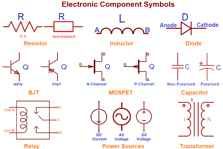
Draw the symbolic representations of NPN and PNP transistors.

There is no leakage current in FET, therefore, the temperature effect on the device is very less or we can say FET is having better thermal stability than BJT.
FET has zero offset voltage, so it can work as an excellent signal chopper because of the zero offset voltage.
MOSFET is an integrated circuit that is fabricated by VLSI designing using planar technology.
In planar technology, the entire MOSFET is fabricated on the same plane.
In N channel MOSFET, the substrate is p-type
In P- channel MOSFET, the substrate is n-type.
In depletion MOSFET, there is a pre-existing channel.
It is widely used as a switch in the digital circuit.
What is a MOSFET? How is it different from a JFET? What are its typical applications?
Metal oxide semiconductor can be operated in both depletion and enhancement modes, but Junction field effect Transistor can be operated in depletion mode only.
It is used as a switch that is faster than a normal diode.
It is used as a rectifier.
It is also used as a clipper or amplitude limiter.
It is used to convert the given sine waveform to a square wave or a pulse waveform.
Define PIV(Peak inverse voltage)?
It is the maximum reverse voltage that can be applied to the Diode. if the voltage across the junction exceeds PIV, under reverse bias condition, the junction gets damaged.Define Reverse saturation current?
It is the current due to the diffusive flow of minority electrons from p- side to N- side, and minority holes from N- side to P- sideWhat is mean by Break down, difference b/w avalanche Break down and Zener Break down?
Avalanche breakdown occurs in PN diode due to impact ionization of electron-hole pair, zener braek down occurs in Zener dioade due to electron hole pair break due to reverse bias voltageWhat are the different breakdown mechanisms on which Zener diode works?
There are 2 types of breakdown mechanisms on which the Zener diode work: Zener breakdown phenomena: is due to large electric field intensity. Occurs at a value less than 6 volts due to tearing or rupturing of covalent bonds in the depletion layer. This is a very sharp breakdown. It occurs in highly doped diodes.Avalanche breakdown mechanism: it is due to electron multiplication which occurs due to multiple collisions between electrons and ions in the depletion layer. It is due to impact ionization. It will occur for a voltage greater than 6 volts and it is not very sharp. This effect occurs in the light-doped reverse bias of the Zener diode.What is transistor?
In electronics, a transistor is a semiconductor device commonly used to amplify or switch electronic signals. The transistor is the fundamental building block of computers, and all other modern electronic devices. Some transistors are packaged individually but most are found in integrated circuits.A junction transistor is simply a sandwich of one type of semiconductor material between two layers of the other type. A transistor is a three terminal current sensing device. It can be looked upon as two pn junction placed back to back. The three terminals are named as emitter base & collector.
What is BJT, explain about its terminals, what are types, and which type is better, why?
Bipolar junction Transistor in this current flows due to two polarities(electrons, holes), NPN or PNP type ,NPN is best because mobility of electrons is more than mobility of holes so electron current is more.What are the different configurations of transistor?
a) Common Emitter (CE) b) Common Base (CB) c) Common collector (CC)What is Common Base configuration?
base is common between input and output circuits. emitter-base terminal input signal is applied and in collector-base terminal output is taken from it.What are the characteristics of CB?
since it has a low input resistance and a high output resistance, current gain of less than 1. The input and output signals in the common-base circuit are in phaseWhat is transistor and why it is called like that?
Because it transfers the input signal from low resistance to high resistanceExplain the physical structure of a BJT?
One N type material is sandwiched between two P type materials or One P type material is sandwiched between two N type materials , widths (C>E>B), doping concentration(E>C>B)Draw the symbolic representations of NPN and PNP transistors.
Which type of amplifier is best BJT or FET and why?
BJT amplifiers are most commonly used in comparison to FET amplifiers because the gain-bandwidth product of BJT is greater than the gain-bandwidth product of FET.What are the important features of FET in comparison to BJT?
FET is a majority carrier device it has no minority careers, unlike BJT, hence it is a less noise noisy device.There is no leakage current in FET, therefore, the temperature effect on the device is very less or we can say FET is having better thermal stability than BJT.
FET has zero offset voltage, so it can work as an excellent signal chopper because of the zero offset voltage.
What do you know about MOSFET?
Metal oxide semiconductor field-effect transistor- it is also known as a voltage-controlled capacitor.MOSFET is an integrated circuit that is fabricated by VLSI designing using planar technology.
In planar technology, the entire MOSFET is fabricated on the same plane.
In N channel MOSFET, the substrate is p-type
In P- channel MOSFET, the substrate is n-type.
In depletion MOSFET, there is a pre-existing channel.
It is widely used as a switch in the digital circuit.
What is a MOSFET? How is it different from a JFET? What are its typical applications?
Metal oxide semiconductor can be operated in both depletion and enhancement modes, but Junction field effect Transistor can be operated in depletion mode only.


Post a Comment
0 Comments